Spark plasma sintering of boron carbide: A revolutionary "black technology" breakthrough in traditional sintering.


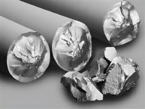
In the field of materials science, boron carbide (B4C), known as "black diamond" due to its high hardness, low density, wear resistance, and neutron absorption capacity, is widely used in high-end fields such as bulletproof armor, nuclear industry, and aerospace. However, traditional sintering processes (such as pressureless sintering and hot pressing sintering) face challenges such as high sintering temperatures, long sintering times, and easy grain coarsening, limiting further improvements in boron carbide performance. In recent years, spark plasma sintering (SPS) technology, with its low temperature, rapid speed, and high efficiency, has become a hot research area for boron carbide, reshaping the application boundaries of this superhard material.


I. SPS Technology: A Revolutionary New Paradigm for Sintering


SPS technology achieves rapid densification of boron carbide through the synergistic effect of pulsed current, mechanical pressure, and thermal field. Its core principle lies in:


Plasma activation: Pulsed current generates instantaneous high-temperature plasma in the interparticle gaps, removing surface oxides and promoting atomic diffusion.


Joule heating and temperature gradient: The electric current generates Joule heating through the graphite mold, and the temperature rises rapidly (up to 600℃/min), forming a temperature gradient that accelerates densification and inhibits grain growth.


Electric Field Assisted Diffusion: The electric field lowers the sintering activation energy, enabling boron carbide to achieve high density (>95%) at 1700-2100℃, which is 300-500℃ lower than the traditional process.


Compared with traditional sintering, boron carbide prepared by SPS has finer grains (nano to micron scale) and superior mechanical properties. For example, at 1600℃ and 300MPa high pressure, the fracture toughness of boron carbide prepared by SPS is increased to 5.56MPa・m¹/², and the dynamic toughness is significantly enhanced.


II. Technological Breakthrough: The Key Leap from Laboratory to Industrialization


1. Parameter Optimization and Microstructure Control


Temperature and Pressure Synergy: Research has found that at low temperatures (1700-2000℃), particle boundary sliding primarily leads to densification, while at high temperatures (>2000℃), dislocation climb is dominant. By precisely controlling the heating rate and pressure, grain size can be accurately controlled from 4μm to the nanometer scale.


Innovative Applications of Sintering Aids: Adding additives such as Al, SiC, and graphene can further optimize performance. For example, B4C/SiC/Al multiphase ceramics with 1.5% graphene (GPLs) show a 25.6% increase in fracture toughness and a 99% increase in flexural strength.


2. One-step fabrication of functionally graded materials


The Napo Materials team has achieved, for the first time, one-step sintering of B4C/Al functionally graded materials using SPS technology. This material achieves a gradient transition from pure B4C (hardness 32 GPa) to pure Al (hardness 1 GPa), successfully solving the problems of large melting point differences and easy formation of impurity phases in traditional processes, providing new ideas for bulletproof armor and high thermal conductivity composite materials.


3. Performance Breakthrough in Extreme Environments


In the nuclear industry, SPS-prepared B4C neutron absorbers achieve a purity of 99.9%, exhibit excellent radiation resistance, and have waste disposal costs that are only one-fifth of those of traditional cadmium-based materials. In the aerospace industry, boron carbide/aluminum composite materials reduce the weight of turbofan engine leading-edge protection plates by 40% and improve fuel efficiency by 2.3%.

  • #
  • #
  • #


III. Industry Prospects: A New Blue Ocean in a Trillion-Dollar Market


1. Applications are flourishing across all fields.


Defense and Military Industry: The U.S. military's Osprey transport aircraft uses B4C composite armor, which reduces weight by 40% and provides protection superior to traditional steel armor.


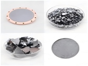
Semiconductors and Electronics: Boron carbide wafer stage flatness error < 1μm, meeting the ultra-high precision requirements of EUV lithography machines. Zhihe New Materials' low-temperature sintering technology reduces the B4C sintering temperature to 1950℃, driving its application in the semiconductor polishing pad field.


New Energy and Environmental Protection: Boron carbide nozzles extend the lifespan of high-pressure sandblasting equipment from 3 months to 2 years, reducing maintenance costs by 80%. Their application in nuclear energy, solar cells, and other fields is also rapidly expanding.


2. Market Size and Policy Dividends


The global boron carbide market is projected to grow from $180 million in 2025 to $320 million in 2030, representing a CAGR of 9.5%. As the world's largest producer, China is seizing the industry's leading position through policy support and technological breakthroughs.


Spark plasma sintering (SPCS) technology is leading boron carbide materials from the laboratory to industrialization. Its superior performance in hardness, thermal stability, and neutron absorption provides disruptive solutions for defense, energy, and electronics. With technological advancements and policy support, boron carbide, this "black diamond," will undoubtedly shine in even more applications, becoming one of the key materials driving human technological progress.


Gold mining high purity boron --- UrbanMines Tech. Material solutions and technical specifications white paper


As a leading company in the field of boron materials in China, UrbanMines Tech. Co., Ltd. focuses on the research development and production of high-purity crystalline boron, amorphous boron, and electronic-grade boron nitride. Relying on years of technological accumulation and a complete process control system, the company's products are exported to high-end markets such as Germany, the United States, Japan, and South Korea, providing core material solutions for semiconductors, new energy, nuclear industry, special alloys, and other fields.


---


Core product and technology advantages

1. Crystalline boron series

- Ultra-high purity crystalline boron (grade 6N, 99.9999%)

Used as a dopant for semiconductor single-crystal silicon rods to ensure chip-level purity requirements.

- High-purity crystalline boron (2N~5N grade)

Used as high-temperature resistant alloy additives and nuclear reactor shielding materials to improve the performance limits of materials.


2. Amorphous boron series (below 5N grade)

It is suitable for solid rocket propellants, high-energy fuel combustion aids, and solar electronic slurries, providing stable energy release characteristics.


3. Electronic grade boron nitride (purity ≥99%)

- Zero magnetism & no black spots: meet the cleanliness requirements of precision electronic devices

- Nano-level particle size control: D50 particle size as low as 10 microns (customizable)

- Excellent thermal conductivity and insulation: suitable for high-frequency electronic packaging and thermal conductive interface materials.


---


Customized technical capabilities

Based on the exclusive process know-how, the company provides a full range of customized services:

✅ Precise control of B11 isotope abundance

✅ Customized particle size classification (nano to micron)

✅ Purity range is adapted as needed (2N~6N)


---


Technical Specifications (Unification of Testing Standards)

To eliminate detection differences and ensure consistency in quality judgment, the following specifications are formulated:


  1. Particle size testing standards
Method Principles and limitations  Company regulations 
Scanning electron microscope Surface morphology observation, unable to statistically distribute; agglomeration is easy to misjudge  Not recommended as a basis for particle size acceptance
Laser particle size analyzer   International general standard, sodium pyrophosphate dispersion + ultrasonic deagglomeration The only recognized test method 

Case description: A Korean customer required an amorphous boron particle size of 2~4μm. The electron microscope misjudged the agglomerated particles as unqualified, and the laser method verified that the particles met the standard.

Specification requirements: Customers need to specify the D50/D90 indicators and use a laser particle size analyzer for testing.


2. Purity Testing Standards

Method Detection range Reasons for differences in results Company regulations
ICP  15 impurities (<1ppm) Few items, low total impurity calculation value 6N purity (99.9999%)
GDMS 70 impurities (<10ppm) Many items, high total impurity calculation value 4N purity (99.99%) 


Core conclusions:

- Physical purity consistency: The same sample may have different nominal purity due to varying numbers of test items, but the actual composition does not change.

- Specification requirements: The customer needs to declare the test method and the number of impurities. Our company will synchronize the test process and attach the original report.


---


Quality Commitment

UrbanMines Tech. Controls the entire process:

* Particle size control: laser particle size analyzer + standardized dispersion process

* Purity control: multi-method cross-validation + ultra-clean production environment

* Isotope control: B11 abundance precision adjustment technology

Continue to provide customers with customizable, highly consistent, and zero-controversy boron material solutions.


---


Conclusion

Deeply cultivating the technology in the field of "boron" and solving the ultimate challenges of materials. UrbanMines Tech. Helps global partners achieve technological innovation and quality leaps with transparent data testing specifications and internationally leading customization capabilities.


---

Boron: From Basic Material to High-Tech Core - Analyzing the Precision Application of High-Purity Boron in Semiconductors and Advanced Fields


In high-tech fields that pursue microscopic limits and pinnacle performance, certain fundamental elements play a crucial role. Boron, element symbol B, atomic number 5, is one such element. This metalloid, found only in compounds in nature, has become an indispensable "key element" in fields such as semiconductors, advanced materials, and the nuclear industry due to its unique electronic structure and physical and chemical properties.


1. "Master Craftsmen" of the Semiconductor Industry: Precision Doping and Crystal Growth


In the semiconductor industry, the value of high-purity crystalline boron lies in its unparalleled precision control capabilities.


The cornerstone of P-type doping: Boron's core use is as a P-type dopant. Silicon (Si) is the undisputed workhorse of semiconductor materials, but inherently it conducts poorly. When boron atoms are precisely introduced into the silicon lattice through techniques such as ion implantation or high-temperature diffusion, boron's outermost shell contains only three electrons, compared to silicon's four electrons. This creates a "hole" that can accommodate and carry electrons, effectively creating a P-type semiconductor. This "doping" process is fundamental to the construction of the PN junction—the fundamental building block of all semiconductor devices, including diodes, transistors, and thyristors.


The key to power devices and scaling: In power devices that must withstand high voltages and high currents (such as IGBTs and power MOSFETs), boron-doped silicon wafers (typically in the high-resistance region) effectively regulate the electric field distribution and enhance the device's withstand voltage. Furthermore, at advanced process nodes, the formation of ultra-shallow junctions requires extremely high doping precision. Boron, due to its small atomic radius, enables finer doping control, meeting the demands of nanoscale devices.


Source material for single crystal growth: In addition to doping, crystalline boron is also used as a source material for growing boron-doped silicon single crystals via the melt process. This method produces silicon ingots with uniform P-type conductivity across the entire wafer, providing the foundation for the large-scale manufacturing of highly consistent semiconductor devices.


2. Beyond Semiconductors: Boron's Outstanding Performance in Multiple Fields


Boron's uses go far beyond semiconductors; its compounds and isotopes shine in many advanced fields.


Advanced Structural Materials: Boron's extremely high hardness (Mohs hardness 9.5) makes it an ideal material for reinforcement. Boron fibers and boride ceramics are key components in the manufacture of high-strength, lightweight composite materials, widely used in aerospace, high-performance sports equipment, and other fields.


Specialty Glass and Ceramics: In glass manufacturing, the addition of boron oxide significantly reduces the coefficient of thermal expansion, imparting excellent thermal shock resistance. This borosilicate glass is a preferred choice for laboratoryware (such as heat-resistant beakers) and high-end cookware. Similarly, the addition of boron compounds to ceramics improves their thermal stability and mechanical strength.


Neutron capture and the nuclear industry: Natural boron contains approximately 20% of the boron-10 isotope, which has an extremely high capture cross section for thermal neutrons. This property makes boron-10 (usually in the form of boron carbide or boric acid) an indispensable control rod material, neutron shielding material, and safety agent for emergency shutdown systems in nuclear reactors.


Organic Synthesis and Pharmaceuticals: In the fine chemical and pharmaceutical fields, boron-containing reagents (such as boronic acids and boronic esters) are important intermediates for building carbon-carbon and carbon-heteroatom bonds, particularly in Suzuki-Miyaura coupling reactions. An increasing number of boron-containing organic molecules are being developed as new pharmaceuticals. For example, certain proteasome inhibitors have become important anti-cancer therapies.

  • #
  • #
  • #


3. Quality is the cornerstone of technology: reliable supply from China


Faced with such extensive and demanding high-tech applications, the requirements for the purity, consistency and specific form (such as particle size and crystal form) of boron materials have reached unprecedented levels.


UrbanMines Tech., a leading manufacturer and supplier of high-purity boron materials in China , deeply understands the crucial impact of material properties on downstream products. Leveraging our proprietary and controlled production lines, we specialize in providing semiconductor-grade high-purity crystalline and amorphous boron, as well as various customized boron compounds, to customers worldwide.


We firmly believe that only the ultimate products can meet the demands of cutting-edge technology. Therefore, we are committed to working closely with global R&D and manufacturing partners to jointly push the boundaries of technology, from chips to clean energy, by providing high-performance, stable and reliable boron material solutions.


keyboard_arrow_up